

Mobile phones, flat panel displays, blu-ray discs and other products utilizing the results derived from electrical and electronic engineering as well as applied physics are everywhere around us. In this faculty we offer fundamental education in the fields of electrical and electronic engineering and applied physics that will form a basis for various industrial fields, including many which relate to familiar electronic, communications and information devices. We also conduct the research and development of advanced technologies with the aim of creating a new technology paradigm for the next generation. Through education and research in electrical and electronic engineering and applied physics, our faculty develops excellent specialists that combine highly specialized knowledge and practical skills with a high standard of ethics. We hope they will help realize the development of a society of highly advanced technology through steady technological development. Our goal is to create technology that paves the path to a hopeful future through our insatiable pursuit of “knowledge”.

Nanomaterial Science and Engineering
Our goal is to elucidate the optical properties and create new functions in regards to semiconductor colloidal quantum dots.
Prof. KIM DaeGwi
Synthesis and optical properties of colloidal quantum dots
In semiconductor quantum dots (QDs) with sizes smaller than 10 nm, quantum effects arise because of the finite size of the QDs. As a result, the QDs exhibit physical/chemical properties and functions different from those of bulk crystals. Thus, semiconductor QDs are considered as a promising new functional material.
In our laboratory, we are designing and manufacturing original semiconductor colloidal QDs, investigating their properties, unraveling new principles and discovering new functions. The breakthrough in synthesizing a new class of colloidal QDs has led to an explosive increase of QD studies as well as having opened up possibilities for various applications, such as biomolecular imaging, QD lasing, QD solar cells, and more.
Pursue new possibilities with colloidal QDs
QD super lattices, in which the QDs are regularly arranged, have the potential to provide new optical properties and functions based on the interactions between adjacent QDs. Two types of interactions occur between adjacent QDs: excitation energy transfer (ET) from small-sized QDs to large QDs and quantum resonance between QDs with equal eigenenergies. Since ET and resonant interactions strongly depend on the distance between the QDs, it is critical to precisely control the distance between QDs to clarify their interaction mechanism. The layer-by-layer (LBL) method can be used to control the distance between QDs because (1) it is possible to laminate QDs dispersed in an aqueous solution on a substrate layer by layer, and (2) the interlayer distance can be controlled by the thickness of the spacer (electrolyte polymer) layer.
We realized precise control of the interlayer distance in quantum dot stacking structures by using the LBL method and clarified the mechanism of ET and quantum resonance between quantum dots for the first time. We believe that our findings have a major impact on how to design and synthesize hyper-structured materials composed of nanomaterials with nano space as well as provide new insight into their photovoltaic properties, which disordered 2D QD films as well as 3D superlattices with long-range inter-QD distances, do not exhibit.
Applied Physics and Electronics Research Areas
Optical Functions Engineering
We are researching optical properties and functions of condensed matter, photonic engineering and wave physics with the goal of creating new optical functions.
In particular, in regards to optical properties and functions of condensed matter and photonic engineering, we focus on various semiconductor thin film based structures (quantum wells, superlattices, etc.) on the nanometer scale where wave properties (quantum properties) of electrons appear in materials. Our advanced research is focused mainly on optical properties and functions such as light emission mechanisms and ultrafast optical responses. In the field of wave physics engineering, we are researching fundamental technologies related to light and terahertz electromagnetic waves as well as engineering applications for terahertz optical elements and new function sensing.
Optical Properties and Functions of Condensed Matter
Our research work is focused on the optical properties and functions of nanoscale film structures and quantum structures (structures in which wave properties of electrons and holes appear) in semiconductors. Semiconductor nanoscale film structures are prepared using various physical vapor growth methods. We conduct advanced research into the various states of energy as well as the light emission mechanisms of the electron systems with the goal of developing guidelines to create new optical functions.

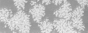
- Plasma emission in the preparation process (pulsed laser ablation) of oxide semiconductor ZnO nanoscale film
Photonic Engineering
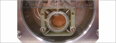
Laser light is playing an active role in familiar devices, such as light sources used in CD readers. These are used to create femtosecond pulse lasers [pulse width: 1-100 fs (from 10^(-15) to 10^(-13) seconds)]. The largest distance the light can travel during a single femtosecond is only 3 viruses (0.3 m). In this field, our research is mainly focused on studying the advanced mechanisms behind the generation of terahertz electromagnetic waves using this light.
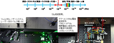
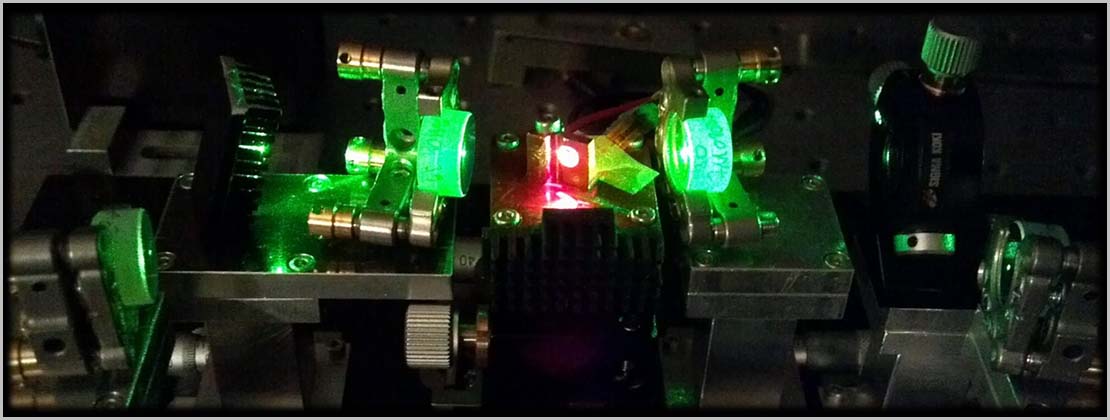
- Terahertz spectroscopy system
Physical Wave Engineering
There are many phenomena occurring constantly around us related to waves and vibrations, as well as many things which use these phenomena. We research the movement of electrons in regards to Light (lasers), terahertz waves, Plasmon and other electromagnetic waves, in regards to wave properties. We are working on creating new technologies combing usage of both light and electrons by understanding their combined behavior and function.
- Scanning electron microscope image of terahertz optical element fabricated by laser lithography
Material Functions Engineering
We are conducting theoretical and practical research into materials and measurement technologies with the goal of realizing new functions. Specifically, we are researching the manufacturing and optical properties of semiconductor nanoparticles (nanomaterial engineering), conducting fundamental and practical research (control of physical properties) based on crystal engineering, vacuum engineering, surface science, the technology for ultra-precision measurementation of surface adsorption / desorption (applied spectroscopy), measurement technology for high speed / high energy particles (physical property detectors), as well as conducting theoretical research to determine the laws and universal principles among diverse and complicated phenomena (Mathematical Engineering). We also actively engage in projects, both originating from the university and from other collaborations between the university and various industries.
Nanomaterial Science and Engineering
We are researching the optical properties and functions of semiconductor quantum dots (colloidal quantum dots) prepared by a hydrothermal method. We aim to understand the photoluminescence mechanism for quantum dots and apply it to new light-emitting materials.
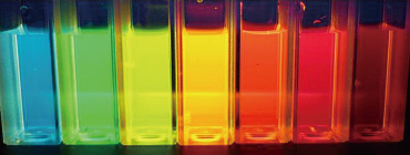
- Colloidal quantum dots exhibiting intense photoluminescence
Mathematical Physics
Mathematical Engineering explores laws and universal principles that are hidden behind diverse and complicated phenomena. We are studying the state of quantum entanglement with group theory as well as engaging in research on metal-insulator transitions and magnetic transitions using the laws of the microscopic world. We are also researching nonlinear and non-equilibrium phenomena.
Design of Material Properties
Using an ultra-high vacuum scanning tunneling microscope (UHV-STM), we can observe at the atomic level thin films and metal silicides of copper and nickel, familiar materials used in coins and other objects. We are also conducting fundamental research in regards to transistors and transparent conductive films made from organic semiconductors and which are fabricated on plastic substrates.
-
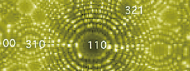
An STM image of a small amount of silicon deposited on a nickel (111) surface
Scan range: 200nm×200nm
Advanced Spectroscopy and Measurements
We explore novel probe beam technologies used in ultra-precise measurements of surface dynamic processes, such as adsorption, desorption, diffusion and ionization on an atomic scale. We also attempt to develop new methods of surface analysis by controlling the spin state of electrons involved in the ionization process at the interface, or by utilizing a focused ion beam.
- Arrangement of surface atoms at the tip apex of the W metal observed using a field ion microscope (FIM)
Particle Detector
Piezoelectric materials generate electricity when deformed or bent by external forces. The properties of these materials allow their application as sensitive elements, even in an environment with limited electric power. Currently, we are researching measurement technology for high-speed and high-energy particles using these materials.
- Ring shaped, high energy particle observation device made from piezoelectric material.
Researchers
*Click to view researcher profiles
-
Prof.
KIM DaeGwi -
Prof.
TERAI Akira -
Assoc. Prof.
SHIBUTA Masahiro -
Assoc. Prof.
SUGITA Ayumu -
Assoc. Prof.
FUKUDA Tsuneo -
Assoc. Prof.
KOBAYASHI Ataru -

RA
TANAKA Kenji
Energy Functions Engineering
We promote research on highly efficient energy generation as well as the conversion and application of energy. In the fields of energy generation and conversion, we study the implementation of solar cells with high conversion efficiency and semiconductor devices with high breakdown voltages and high operating speeds, using various methods, such as the bonding of foreign materials (power electronics). We are proceeding a study aiming at realization of highly efficient material processing with reactive plasma and using generated energy (material measurement engineering).
Power Electronics
The study of semiconductor devices on the boundary between science (semiconductor physics) and engineering (electronics). We are researching high efficiency solar cells, which are semiconductor devices that hold a high level of importance in our modern society, as well as wide-gap semiconductor devices.
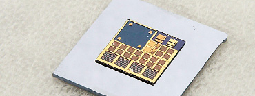
- Tandem solar cells manufactured by bonding technology
Electronic Materials and Measurements
We are working on the synthesis of new functional materials, the modification and analysis of existing materials which utilize plasma states in which atoms and molecules are ionized, and on the development of technologies for functional improvement and modification of certain materials. We are also developing technology to improve the stability of unstable organic semiconductor thin films by forming them using a method based on plasma polymerization.

- Plasma generated in ethanol solution for hydrocarbon reforming
Researchers
*Click to view researcher profiles
-
Prof.
SHIGEKAWA Naoteru -

Prof.
SHIRAFUJI Tatsuru -

Prof.
OH Jun-Seok -
Prof.
(Cross Appointment)
TAKAOKA Motoko -
Lecturer
LIANG Jianbo -
Assoc. Prof.
TAKECHI Seiji -

Lecturer
MURAJI Masafumi
Admission Policy
The Faculty of Applied Physics and Electronics develops a wide range of advanced technologies in the fields of electrical and electronic engineering and applied physics. This faculty fosters engineers and researchers capable of performing advanced multidisciplinary R&D which deals with various electromagnetic phenomena, electronics and semiconductor related engineering, quantum electronics, lasers and solid-state physics, which is the foundation of all these subjects. We are looking for ambitious students meeting the following requirements.
- Those interested in physics, electric and electronic engineering, and who have a deep interest in applying them to a wide range of engineering.
- Those with a strong interest in a wide range of electronic and physical technologies and subjects, such as understanding the physical properties of substances, electricity and light, and experimental and theoretical clarification of their new functions as well as those with a strong desire for autonomous and proactive learning and research.
- Those with desire to find and tackle international issues.
![]()